Research
Overview
Our research is focused on the development of novel optoelectronic devices based on artificially structured materials systems, whose properties can be tailored by design to meet specific applications in a way that is not afforded by simply using bulk materials. Examples include light emitters, modulators, and photodetectors based on bandgap-engineered semiconductor quantum structures, crystalline nanomembranes and 2D materials, and metasurfaces consisting of plasmonic and dielectric nanoantennas. This work is generally aimed at the demonstration of new device concepts with enhanced performance or advanced capabilities compared to the state of the art, guided by relevant applications where optoelectronics plays a central role. Over the past several years, we have addressed key device technology gaps in the areas of optical communications, biochemical sensing, and computational imaging for microscopy and computer vision. Specific activities involve both theoretical and experimental efforts, including design and simulations (often based on the FDTD method for electromagnetic modeling), device micro- and nano-fabrication, and electrical and optical characterization.
Ongoing Projects
Metasurface-enhanced optoelectronics
Photonic metasurfaces (i.e., rationally designed two-dimensional arrays of metallic or dielectric nanoparticles) are currently revolutionizing the design and development of optical components for multiple applications of light-based technologies. Traditionally, metasurfaces are designed to shape the wavefronts of free-space radiation according to a desired passive device operation (e.g., light focusing, polarization control, holographic projection). Our recent work has pioneered the integration of similar nanoparticle arrays within the active materials of optoelectronic devices such as LEDs and photodetectors. These devices typically employ external bulk optical elements (e.g., lenses, mirrors, polarizers, and gratings) to interface with free-space radiation, which can dramatically limit their miniaturization, scalability, and portability. The use of integrated metasurfaces allows for similar functionalities with greatly reduced form factor. A particularly significant example is the development of angle-sensitive photodetectors for computational imaging applications such as compound-eye vision with ultrawide field of view, optical spatial filtering to facilitate image classification, and quantitative phase imaging.

- M. Erturan, J. Liu, M. A. Roueini, N. Malamug, L. Tian, and R. Paiella, “Chiral Phase-Imaging Meta-Sensors,” Nanophotonics, vol. 14, pp. 947-957, 2025.
- Liu, H. Wang, Y. Li, L. Tian, and R. Paiella, “Asymmetric Metasurface Photodetectors for Single-Shot Quantitative Phase Imaging,” Nanophotonics, vol. 12, pp. 3519-3528, 2023.
- Kogos, Y. Li, J. Liu, Y. Li, L. Tian, and R. Paiella, “Plasmonic Ommatidia for Lensless Compound-Eye Vision,” Nat. Commun., vol. 11, art. no. 1637, 2020.
- Wang, Y. Li, R. Toufanian, L. C. Kogos, A. Dennis, and R. Paiella, “Geometrically-Tunable Beamed Light Emission from a Quantum-Dot Ensemble Near a Gradient Metasurface,” Adv. Opt. Mater., vol. 8, art. no. 1901951, 2020.
- C. Kogos and R. Paiella, “Light Emission near a Gradient Metasurface,” ACS Photon., vol. 3, pp 243–248, 2016.
Graphene plasmonic devices for THz optoelectronics
Terahertz radiation is technologically significant for multiple imaging applications (e.g., for security screening, medical diagnostics, and industrial process control), as well as future wireless communications beyond 5G. However, the widespread adoption of THz systems for these applications is currently limited by the lack of suitable devices for the generation, modulation, and detection of THz radiation. To address this outstanding technology gap, we are pursuing the use of actively tunable plasmonic resonances in graphene nanoribbons. In particular, we have demonstrated the promise of these nanostructures for the development of THz radiation sources as well as metasurface devices for THz wavefront shaping and beam steering.

- Li, M. R. Krisshnamurthi, W. Luo, A. K. Swan, X. Ling, and R. Paiella, “Graphene Metasurfaces for Terahertz Wavefront Shaping and Light Emission,” Opt. Mater. Express, vol. 12, pp. 4528–4546, 2022 (invited review article).
- Li, K. Tantiwanichapan, A. K. Swan, and R. Paiella, “Graphene Plasmonic Devices for Terahertz Optoelectronics,” Nanophotonics, vol. 9, pp. 1901-1920, 2020 (invited review article).
- Li, P. Ferreyra, A. K. Swan, and R. Paiella, “Current-Driven Terahertz Light Emission from Graphene Plasmonic Oscillations,” ACS Photon., vol. 6, pp. 2562-2569, 2019.
- Tantiwanichapan, X. Wang, H. Durmaz, Y. Li, A. K. Swan, and R. Paiella, “Graphene Terahertz Plasmons: a Combined Transmission Spectroscopy and Raman Microscopy Study,” ACS Photon., vol. 4, pp. 2011-2017, 2017.
Past Projects
Group-IV semiconductor optoelectronics
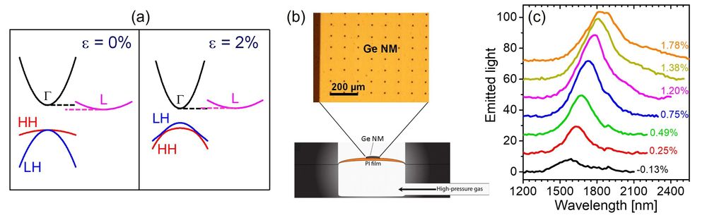
Optoelectronic devices based on silicon and germanium (the leading materials system of microelectronics) have been the subject of extensive research and development for the past few decades, motivated by their potential to enable the monolithic integration of photonic and electronic device functionalities on a CMOS-compatible platform. However, the development of Si/Ge active devices (particularly light emitters) is severely complicated by their indirect energy bandgap, which results in negligibly small radiative efficiency. To address this challenge, we have reported the first demonstration of direct-bandgap germanium capable of providing optical gain at infrared wavelengths. This work leveraged the unique mechanical properties of ultrathin nanomembranes to fulfill a long-standing theoretical prediction of the effect of strain on the Ge band structure. Correspondingly, it opened the way for a new line of research focused on CMOS-compatible group-IV active optoelectronics based on strain engineering.
- Gok, X. Wang, S. Scott, A. Bhat, H. Yan, A. Pattammattel, E. Nazaretski, Y. S. Chu, Z. Huang, R. M. Osgood Jr., M. G. Lagally, and R. Paiella, “Strain-Induced Lateral Heterostructures in Patterned Semiconductor Nanomembranes for Micro- and Optoelectronics,” ACS Appl. Nano Mater., vol. 4, pp. 6160–6169, 2021.
- Boztug, J. R. Sánchez Pérez, F. Cavallo, M. G. Lagally, and R. Paiella, “Strained-Germanium Nanostructures for Infrared Photonics,” ACS Nano, vol. 8, pp. 3136–3151, 2014 (invited review article).
- Boztug, J. R. Sánchez Pérez, F. F. Sudradjat, RB Jacobson, D. M. Paskiewicz, M. G. Lagally, and R. Paiella, “Tensilely Strained Germanium Nanomembranes as Infrared Optical Gain Media,” Small, vol. 9, pp. 622–630, 2013.
- R. Sánchez Pérez, C. Boztug, F. Chen, F. F. Sudradjat, D. M. Paskiewicz, RB Jacobson, M. G. Lagally, and R. Paiella, “Direct-Bandgap Light-Emitting Germanium in Tensilely Strained Nanomembranes,” Proc. Natl. Acad. Sci. USA, vol. 108, pp. 18893–18898, 2011.
Intersubband optoelectronics with novel quantum structures
Intersubband transitions in semiconductor quantum wells (i.e., electronic transitions between quantum-confined states derived from the same energy band) form the basis of well-established device technologies, most notably mid- and far-infrared quantum cascade lasers (QCLs) and quantum well infrared photodetectors (QWIPs) based on arsenide heterostructures. Our work has expanded the reach of intersubband optoelectronics to the emerging families of III-nitride and SiGe quantum wells, with early demonstrations of key device functionalities such as ultrafast all-optical switching for fiber-optic communications, light emission at record short intersubband wavelengths, and THz photodetection. This work also includes two seminal theoretical studies showing the potential of both materials systems to overcome the fundamental limitations of existing THz QCLs for room-temperature operation.

- D. Moustakas and R. Paiella, “Optoelectronic Device Physics and Technology of Nitride Semiconductors from the UV to the Terahertz,” Rep. Prog. Phys., vol. 80, art. no. 106501, 2017 (invited review article).
- Durmaz, P. Sookchoo, X. Cui, RB Jacobson, D. E. Savage, M. G. Lagally, and R. Paiella, “SiGe Nanomembrane Quantum Well Infrared Photodetectors,” ACS Photon., vol. 3, pp. 1978-1985, 2016.
- Sookchoo, F. F. Sudradjat, A. M. Kiefer, H. Durmaz, R. Paiella, and M. G. Lagally, “Strain-Engineered SiGe Multiple-Quantum-Well Nanomembranes for Far-Infrared Intersubband Device Applications,” ACS Nano, vol. 7, pp. 2326-2334, 2013.
- F. Sudradjat, W. Zhang, J. Woodward, H. Durmaz, T. D. Moustakas, and R. Paiella, “Far-Infrared Intersubband Photodetectors based on Double-Step III-Nitride Quantum Wells,” Appl. Phys. Lett., vol. 100, art. no. 241113, 2012.
- Driscoll, Y. Liao, A. Bhattacharyya, L. Zhou, D. J. Smith, T. D. Moustakas, and R. Paiella, “Optically Pumped Intersubband Emission of Short-Wave Infrared Radiation with GaN/AlN Quantum Wells,” Appl. Phys. Lett., vol. 94, art. no. 081120, 2009.
- Bellotti, K. Driscoll, T. D. Moustakas, and R. Paiella, “Monte Carlo Study of GaN Versus GaAs Terahertz Quantum Cascade Structures,” Appl. Phys. Lett., vol. 92, art. no. 101112, 2008.
- Li, A. Bhattacharyya, C. Thomidis, T. D. Moustakas, and R. Paiella, “Ultrafast All-Optical Switching with Low Saturation Energy via Intersubband Transitions in GaN/AlN Quantum-Well Waveguides,” Opt. Express, vol. 15, pp. 17922-17927, 2007.
- Driscoll and R. Paiella, “Silicon-Based Injection Lasers Using Electronic Intersubband Transitions in the L Valleys,” Appl. Phys. Lett., vol. 89, art. no. 191110, 2006.